
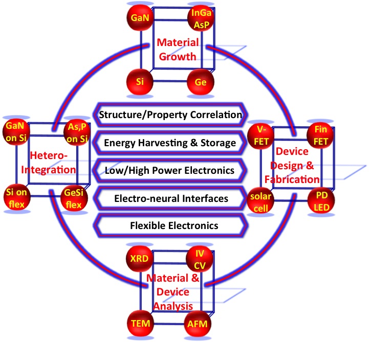
Our research encompasses materials science and device physics for discovering, understanding, and tailoring the physical properties of electronic materials at micro, nano, and atomic scales. We are an experimental group homed by the ECE department at UC San Diego and we conduct both fundamental and applied research with unique expertise that spans materials growth of Ge and Si by CVD, Arsenide, Phosphide, and Nitride compound semiconductors by MOVPE, advanced fabrication of semiconductor devices using these materials for electronics, optoelectronics, energy and power applications, and bio-interface devices and platforms. Our ongoing projects include:
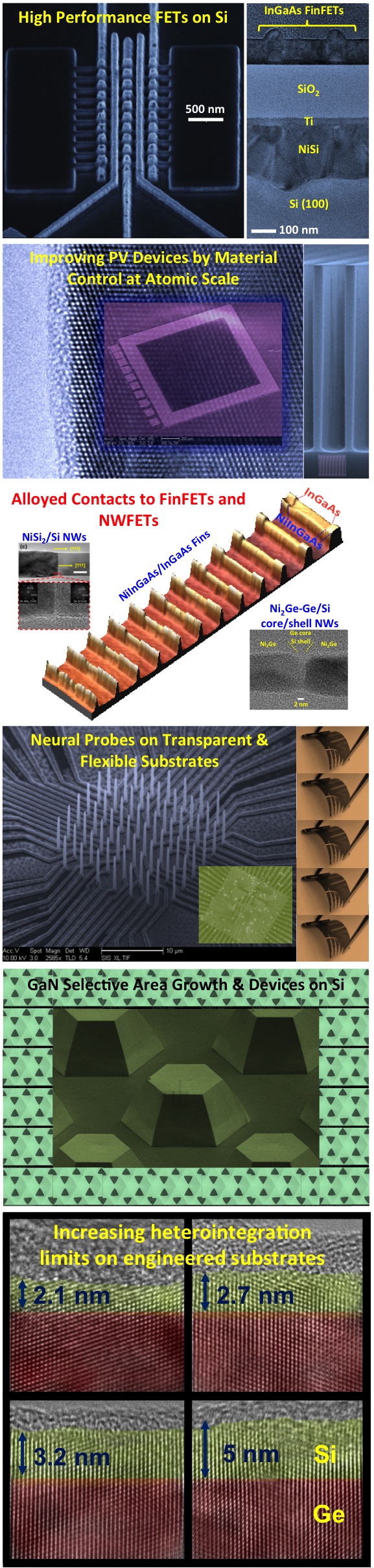
1. Structure-Property Correlation in Nanoscale Materials: A primary theme of our research work is in-situ microscopy of novel nanoscale phenomena using Transmission Electron Microscopy (TEM) at the Center for Integrated Nanotechnologies (LANL/Sandia). Our group has recently discovered a number of novel nanoscale behaviors relevant to solid-state reactions at crystalline boundaries [48] and to electrochemical reactions in bandgap engineered devices [50]. We reported earlier on the alloy reactions between Ni and Ge/Si nano-channels [54] and are currently studying the kinetics, dynamics, and structural behavior of Ni-InGaAs for FinFET geometries. Our unique heterogeneous integration scheme allows us to study metal-semiconductor interactions and other solid-state or electrochemical reactions for a wide variety of geometries. The powerful basic science tools that we are developing are key for enabling future technologies in energy efficient electronics, energy harvesting and storage.
2. Understanding and Controlling the influence of Surfaces in Nanoscale PV Devices: We have previously realized the first epitaxially grown radial Si solar cells with fine control over their doping/absorption profiles by epitaxial growth in CVD in a fab-compatible process [47]. The power conversion efficiencies of these devices was limited to 10%. We are impvoring the performance of our PV devices by understanding and controlling their surface and interface structure, and currently seed advanced thin crystalline and flexible films for efficient and economical energy PV device concepts.
3. Transistor Channels for future Technology Node: We are developing contact and channel technologies that can assist in realizing sub-10 nm channel lengths in future technology nodes. Our work focused in the past on nanowire channels and we are currently bridging the gap between InGaAs FinFETs and future technology nodes on the materials, device, and integration levels. The NiInGaAs has been touted as a self-aligned low resistance ohmic contact to InGaAs channels, but little is known about the interface structural and morphological properties for different orientations and Fin widths. We developed platforms that enable studying these alloy interactions. We also reported the first InGaAs FinFETs on Si substrates by silicide wafer bonding [55]. We are currently pursuing contact engineering for enhanced device performance and have set the grounds for the monolithic integration of III-V channels on Si.
4. GaN for High Power Electronics: We are studing the selective area growth on GaN on Si and were recently successful in growing over 12 micron thick GaN on Si without cracking. We believe that our technology when matured over the high power device level, can be disruptive for high power devices with significant energy saving costs. We are utlizing other novel growth geometires for high power switches. These projects are in collaboration with Profs. Paul K. L. Yu and Prof. Peter M. Asbeck.
5. Electro-Neural Interfaces: We are deeply interested in the development of technologies that are capable of high spatio-temporal mapping and stimulating of neural activity and of simultaneously uncovering details of subcellular processes from a large population of neurons in a neural network. Our devices are projected to have the capacity of targeted and programmable drug delivery, and our integration technology enable multi-modal interfaces at high densities. We have significant efforts on flexible and conformal interfaces that are envisioned to increase the spatiotemporal resolution of neural probes.
6. Flexible Electronics: We have extensive expertise in the development of sensors [1] and electronics on flexible substrates. These devices can be used for health-monitoring and intervention, and our integration scheme allows realization of high speed and bit data rate transmission for wearable electronics.
7. Extending Coherency Limits on Engineered Substrates: There have been many demonstrations in the literature for the growth of heteroepitaxial materials in the nanowire core/shell form. We have developed growth techniques for the in-situ CVD epitaxial growth of crytalline core/shell nanowires without the requirement of chemical and/or thermal treatements [32, 33]. These techniques allowed us to to experimentally demonstrate and measure higher critical thicknesses in the heteroepitaxy of lattice mismatched materials on nanowire 'substrates' [44] for the first time. Our group's efforts are currently tailored toward the growth of III-V compound semiconductor materials on Si through novel approaches and geometries.